


Applications of 3D Laser Profilers in Silicon Wafer Manufacturing | SinceVision
SinceVision has established itself as a leader in cutting-edge sensor technology, particularly in the realm of 3D laser profilers. These advanced measuring instruments play a crucial role in various manufacturing processes, especially within the photovoltaic (PV) industry. This article will delve into the diverse applications of SinceVision's 3D laser profilers, highlighting their significance in ensuring quality control and precision measurement in solar cell production.
Applications in Silicon Wafer Manufacturing
1. Wafer Thickness, Line Mark, and TTV Detection
a. Application Scenario
After the silicon wafer is produced, it needs to be tested by a sorting machine for multiple indicators such as thickness, linear marks, TTV, warpage, etc. to determine whether the silicon wafer meets the set requirements, and then sorted into the corresponding bin box according to the test data, and finally the silicon wafer is sorted into different grades.

Fig: Silicon wafer thickness/line mark/TTV detection
b. Solution
The SR8010 3D laser profiler measuring instrument can perform thickness, TTV, maximum line mark and other tests on various special silicon wafers. The repeatability of the thickness of the measurement items can be within 0.5um, the repeatability of TTV within 1.5um, and the repeatability of line marks within 1.5um. It has ultra-high-profile points and detection speed and can achieve accurate and efficient detection.
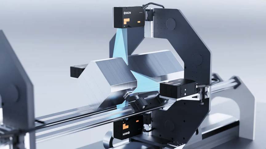
2. Silicon rod size detection
a. Application Scenario
Silicon rods are widely used in the field of solar cell manufacturing due to their excellent performance. After the silicon rods are manufactured, they may have defects such as external cracks, voids, bubbles, internal impurities, etc., so strict quality control tests are required before they can be used in subsequent production

Fig: Silicon rod size detection
b. Solution
The SR7060 3D laser profiler measuring instrument can detect multiple items such as size, arc length, verticality, etc. of silicon rods. It uses multiple measuring instruments to scan and adopts image algorithm stitching technology to form a complete image of the silicon rod, with an item accuracy of 0.02mm.


 Compare
 Clear the comparison bar
