


13th Semiconductor Equipment, Core Components, and Materials Expo | SinceVision to Showcase Advanced Semiconductor Measurement Solutions
SinceVision will present semiconductor precision measurement solutions, including solder ball inspection, wafer edge alignment, and wafer thickness detection, at the 13th Semiconductor Equipment, Core Components, and Materials Expo in Wuxi.
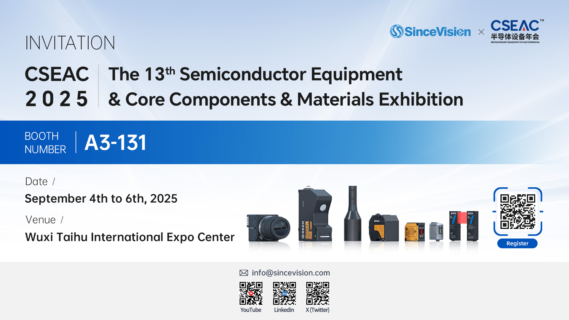


Wuxi, China – September 1, 2025 – SinceVision, a pioneer in industrial sensor innovation, will participate in the 13th Semiconductor Equipment, Core Components, and Materials Expo (CSEAC) at the Wuxi Taihu International Expo Center. At booth A3-131, the company will present its full range of products and precision semiconductor measurement solutions designed to drive the intelligent transformation of semiconductor manufacturing.
As a leader in precision sensing and inspection, SinceVision will demonstrate its classic semiconductor application cases and cutting-edge 3D measurement technologies. The company’s solutions are engineered to deliver accuracy, stability, and speed for semiconductor inspection and production processes.

Featured Applications at the Expo
Chip Solder Ball Height Inspection
Overcomes solder ball reflection interference for reliable results.
One-click indexing for faster and easier operation.
Key specs: Line width 14.5 mm, depth of field 5.2 mm, X spacing 5 μm.
Linearity ±0.02% F.S., frame rate 3200–67000 Hz.

Wafer Edge Alignment
Stable detection of transparent and semi-transparent materials.
High-precision alignment with repeat accuracy of 5 μm.
Key specs: Measurement range 10 mm, frame rate 4000 Hz.
Center deviation ±0.05 mm, angle deviation ±0.1°.

Wafer Thickness Measurement
Thickness accuracy up to 1 μm with temperature drift<0.015% F.S./°C.
Stable through-beam measurement with no offset.
Key specs: Range 1 mm, minimum thickness 30 μm.
Sampling frequency 500–33000 Hz.

Meeting Industry Partners
SinceVision looks forward to engaging with industry professionals and partners at the event. Visitors are invited to discuss future paths for semiconductor manufacturing upgrades, explore new opportunities for high-quality industrial transformation, and experience hands-on demonstrations of SinceVision’s semiconductor solutions.
Event Information
Event: 13th Semiconductor Equipment, Core Components, and Materials Expo
Date: September 4–6, 2025
Location: Wuxi Taihu International Expo Center
Booth: A3-131
SinceVision welcomes all semiconductor industry peers and partners to visit the booth and explore cutting-edge sensing technologies that ensure precision, efficiency, and innovation in semiconductor production.
Book a meeting at info@sincevision.com or click here to receive a ticket.


 Compare
 Clear the comparison bar
