


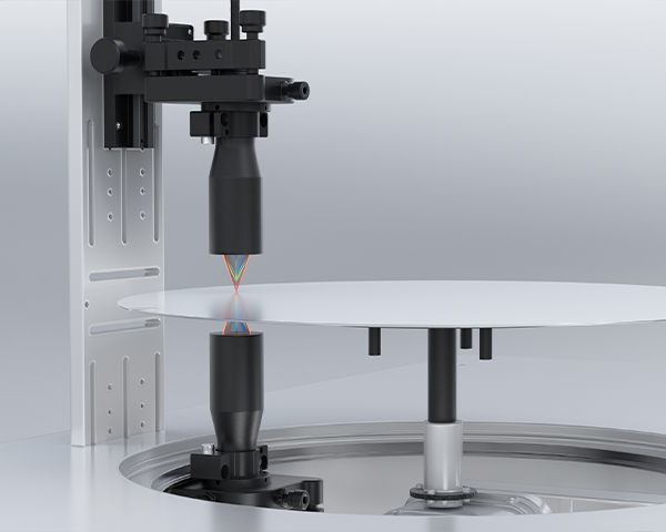
Through-Beam Measurement of Semiconductor Wafer Thickness with Spectral Confocal Displacement Sensor
Through-Beam Measurement of Semiconductor Wafer Thickness with Spectral Confocal Displacement Sensor
 Product Inquiry
Industry pain points and demands
As the foundational substrate for semiconductor chips, the thickness of a wafer plays a pivotal role in determining the chip's performance, reliability, and final yield rate. Accurate wafer thickness measurement ensures manufacturing stability and consistency, which ultimately enhances the overall product quality.
Semiconductor wafer thickness directly influences chip performance and manufacturing consistency, posing several challenges:
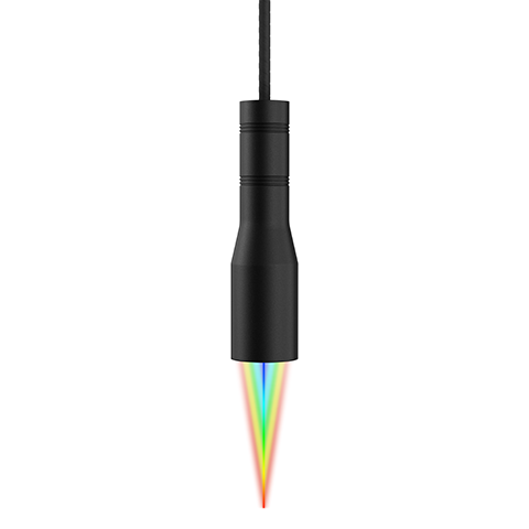
Material Variability: Wafers with diverse thin-film layers, including highly transparent and reflective materials, create unstable signal feedback.
Precision Requirements: Micron-level accuracy is critical for ensuring product quality and yield rates.
Speed: Accurate measurements must be maintained on high-speed production lines.


 Compare
 Clear the comparison bar
