


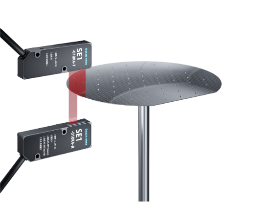
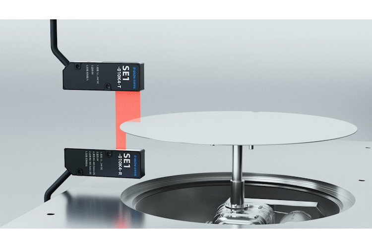
Semiconductor Wafer Center Concentricity and Notch Positioning with Through-Beam Edge Sensor
Semiconductor Wafer Center Concentricity and Notch Positioning with Through-Beam Edge Sensor
 Product Inquiry
Industry pain points and demands
Semiconductor wafers often consist of multiple thin-film layers, each varying in material and structure. The Through-Beam Edge Sensor offers exceptional stability and micron-level accuracy for wafer thickness measurement. It effectively handles a range of materials, including those with high transparency, high reflectivity, low reflectance, or rough textures. This capability addresses challenges like unstable signal feedback caused by different material properties, ensuring reliable and precise measurements across diverse scenarios.
Challenges include:
Center Concentricity: Detecting misalignment of wafer centers with precision can directly impact processing accuracy and yield.
Notch Positioning: Accurate detection of wafer notches ensures proper orientation during processing.
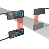
Speed and Accuracy: Modern production lines demand real-time, high-precision sensing solutions to handle high-throughput environments.


 Compare
 Clear the comparison bar
