


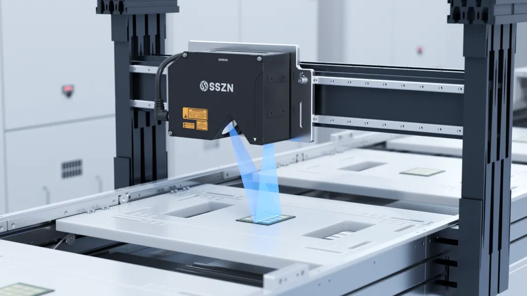
Chip Flatness Inspection with SinceVision 3D Laser Profiler
Chip Flatness Inspection with SinceVision 3D Laser Profiler
 Product Inquiry
Industry pain points and demands
In the semiconductor industry, chip flatness is critical for reliable packaging, manufacturing yield, and performance. However, uneven surfaces pose significant challenges. They can lead to poor solder connections, reduce production yield due to misalignment in flip-chip and SMT processes, introduce mechanical stress causing failures, impair thermal performance in high-power chips, and disrupt advanced packaging technologies like TSVs and micro-bumps.
Additionally, warped chips can cause misalignment in high-speed assembly lines, affecting manufacturing precision. Ensuring flatness is essential to mitigate these issues and enhance overall chip reliability and longevity.


 Compare
 Clear the comparison bar
