


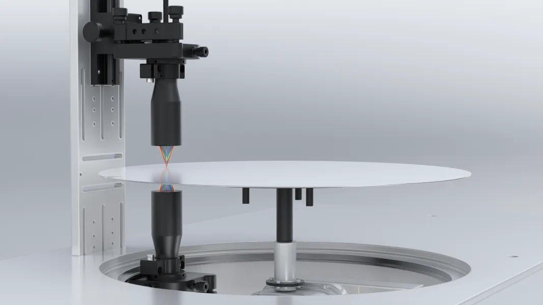
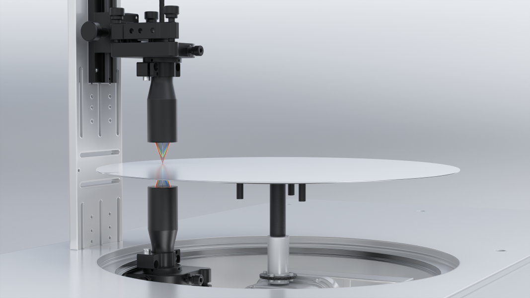
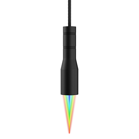
Wafer Thickness Inspection with SinceVision Spectral Confocal Displacement Sensor
Wafer Thickness Inspection with SinceVision Spectral Confocal Displacement Sensor
 Product Inquiry
Industry pain points and demands
As semiconductor technology evolves, the push for larger wafer sizes and superior quality has intensified. Even minor deviations in wafer thickness can disrupt the production process, leading to issues like chip fractures or circuit instability. These imperfections compromise the integrity of the final product, resulting in costly rework or scrapped materials.
Manufacturers require real-time, high-accuracy wafer thickness inspection to maintain consistency, reduce waste, and meet the stringent standards of modern chip fabrication. Without a reliable solution, achieving optimal quality and efficiency remains a significant challenge.


 Compare
 Clear the comparison bar
