


Wafer Thickness, Line Mark, and TTV Detection in Silicon Wafer Manufacturing
Wafer Thickness, Line Mark, and TTV Detection in Silicon Wafer Manufacturing
 Product Inquiry
Industry pain points and demands
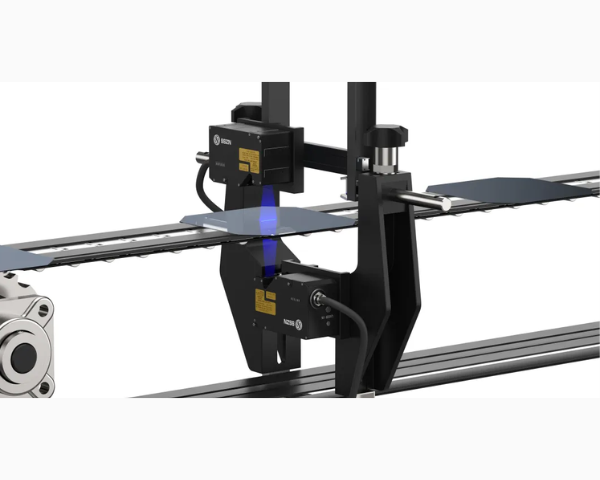
After the silicon wafer is produced, it needs to be tested by a sorting machine for multiple indicators such as thickness, linear marks, TTV, warpage, etc. to determine whether the silicon wafer meets the set requirements, and then sorted into the corresponding bin box according to the test data, and finally the silicon wafer is sorted into different grades.
Key challenges include:
Thickness Variation: Even slight deviations in wafer thickness can affect performance and production efficiency.
Line Mark and TTV Defects: Linear marks and high total thickness variation (TTV) reduce wafer quality and usability.
High-Speed, High-Accuracy Testing: Traditional methods often fail to meet the speed and precision required for sorting wafers into grades.


 Compare
 Clear the comparison bar
